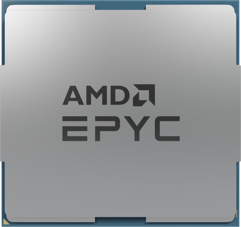
AMD EPYC 9745 128 Cores 256 Threads 400 W TDP 2.4 GHz Frequency 3.7 GHz Boost Turin Codename Socket SP5
$12,999.00 Original price was: $12,999.00.$12,141.00Current price is: $12,141.00.

AMD EPYC 9655 96 Cores 192 Threads 400 W TDP 2.6 GHz Frequency 4.5 GHz Boost Turin Codename Socket SP5
$12,999.00 Original price was: $12,999.00.$11,852.00Current price is: $11,852.00.


AMD EPYC 9655P 96 Cores 192 Threads 400 W TDP 2.6 GHz Frequency 4.5 GHz Boost Turin Codename Socket SP5
AMD EPYC 9655P 96 Cores 192 Threads 400 W TDP 2.6 GHz Frequency 4.5 GHz Boost Turin Codename Socket SP5
$10,999.00 Original price was: $10,999.00.$10,811.00Current price is: $10,811.00.
Guaranteed Safe Checkout

Features & Compatibility
The AMD EPYC 9655P is a server/workstation processor with 96 cores, launched in October 2024, at an MSRP of $10811. It is part of the EPYC lineup, using the Zen 5 (Turin) architecture with Socket SP5. Thanks to AMD Simultaneous Multithreading (SMT) the core-count is effectively doubled, to 192 threads. EPYC 9655P has 384 MB of L3 cache and operates at 2.6 GHz by default, but can boost up to 4.5 GHz, depending on the workload. AMD is building the EPYC 9655P on a 4 nm production process using 99,780 million transistors. The silicon die of the chip is not fabricated at AMD, but at the foundry of TSMC. The multiplier is locked on EPYC 9655P, which limits its overclocking capabilities.
With a TDP of 400 W, the EPYC 9655P is extremely power hungry, which means you need top-notch cooling. AMD’s processor supports DDR5 memory with a twelve-channel interface. The highest officially supported memory speed is 6000 MT/s, but with overclocking (and the right memory modules) you can go even higher. ECC memory is supported, too, which is an important capability for mission-critical systems, to avoid data corruption. For communication with other components in the system, EPYC 9655P uses a PCI-Express Gen 5 connection. This processor lacks integrated graphics, you might need a graphics card.
Hardware virtualization is available on the EPYC 9655P, which greatly improves virtual machine performance. Programs using Advanced Vector Extensions (AVX) will run on this processor, boosting performance for calculation-heavy applications. Besides AVX, AMD has added support for the newer AVX2 and AVX-512 instructions, too.
Physical
| Socket: | AMD Socket SP5 |
|---|---|
| Foundry: | TSMC |
| Process Size: | 4 nm |
| Transistors: | 99,780 million |
| Die Size: | 12x 70.6 mm² |
| I/O Process Size: | 6 nm |
| Package: | FC-LGA6096 |
Processor
| Market: | Server/Workstation |
|---|---|
| Production Status: | Active |
| Release Date: | Oct 10th, 2024 |
| Launch Price: | $10811 |
| Part#: | 100-000001522 |
Performance
| Frequency: | 2.6 GHz |
|---|---|
| Turbo Clock: | up to 4.5 GHz |
| Base Clock: | 100 MHz |
| Multiplier: | 26.0x |
| Multiplier Unlocked: | No |
| TDP: | 400 W |
| Configurable TDP: | 320-400 W |
Architecture
| Codename: | Turin |
|---|---|
| Generation: | EPYC (Zen 5 (Turin)) |
| Memory Support: | DDR5 |
| Rated Speed: | 6000 MT/s |
| 2DPC Rated Speed: | 4400 MT/s |
| Memory Bus: | Twelve-channel |
| ECC Memory: | Yes |
| PCI-Express: | Gen 5, 128 Lanes (CPU only) |
| CXL: | Gen 2.0 |
Core Config
| # of Cores: | 96 |
|---|---|
| # of Threads: | 192 |
| SMP # CPUs: | 1 |
| Integrated Graphics: | N/A |
Cache
| Cache L1: | 80 KB (per core) |
|---|---|
| Cache L2: | 1 MB (per core) |
| Cache L3: | 384 MB (shared) |
Features
|
Notes
| CXL 2.0 supports Type 3 devices which can provide significant increases to system attached DRAM capacity. SEV-SNP security features extend to Type 3 devices.
AMD’s “Turin” CPUs can be configured for DDR5 6400 MT/s with 1 DIMM per channel (1DPC) in specific scenarios, but 6000 MT/s is the official supported rating for the SP5 platform with firmware updates provided. |
Additional information
Customer Reviews
Be the first to review “AMD EPYC 9655P 96 Cores 192 Threads 400 W TDP 2.6 GHz Frequency 4.5 GHz Boost Turin Codename Socket SP5” Cancel reply
Related Products
NVIDIA RTX 5000 Ada Generation 32GB
$4,860.00 – $5,730.00Price range: $4,860.00 through $5,730.00
Select options
This product has multiple variants. The options may be chosen on the product page
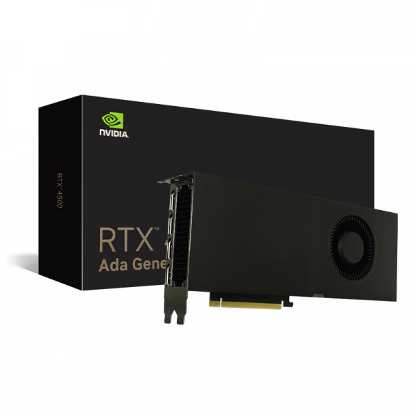
NVIDIA RTX 4500 Ada Generation 24GB
$2,743.00 – $2,916.00Price range: $2,743.00 through $2,916.00
Select options
This product has multiple variants. The options may be chosen on the product page
NVIDIA RTX A6000 48GB
$5,000.00 – $8,500.00Price range: $5,000.00 through $8,500.00
Select options
This product has multiple variants. The options may be chosen on the product page
NVIDIA RTX A1000 8GB
$469.00 – $520.00Price range: $469.00 through $520.00
Select options
This product has multiple variants. The options may be chosen on the product page
NVIDIA RTX A400 4GB
$208.00 – $225.00Price range: $208.00 through $225.00
Select options
This product has multiple variants. The options may be chosen on the product page





 Blade Servers
 GPU Servers
 Supermicro GPU Server
 ASUS GPU Server
 Gigabyte GPU Server
 Inspur GPU Server
 other server
 Storage Servers
 Twin Servers
 Dell workstation
 HP workstation
 Lenovo workstation
 Supermicro workstation
 Inspur workstation
 ASUS workstation
 Nvidia workstation
 Gigabyte workstation
 IBM workstation
 AMD server Processors
 intel server Processors
 Mechanical hard drive
 HPE Mechanical hard drive
 Seagate Mechanical hard drive
 TOSHIBA Mechanical hard drive
 NVME Solid State Drive
 Samsung NVME Solid State Drive
 Kingston NVME Solid State Drive
 Hynix SK NVME Solid State Drive
 Micron NVME Solid State Drive
 Colorful NVME Solid State Drive
 Crucial NVME Solid State Drive
 KIOXIA NVME Solid State Drive
 PNY NVME Solid State Drive
 Others NVME Solid State Drive
 Sata Solid State Drive
 Samsung Sata Solid State Drive
 Kingston Sata Solid State Drive
 Micron Sata Solid State Drive
 Hynix SK Sata Solid State Drive
 Colorful Sata Solid State Drive
 Crucial Sata Solid State Drive
 KIOXIA Sata Solid State Drive
 PNY Sata Solid State Drive
 Other Sata Solid State Drive
 Nvidia Graphics Cards
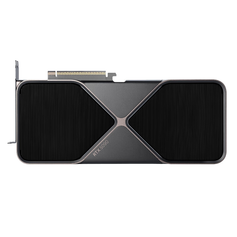 RTX 50 series
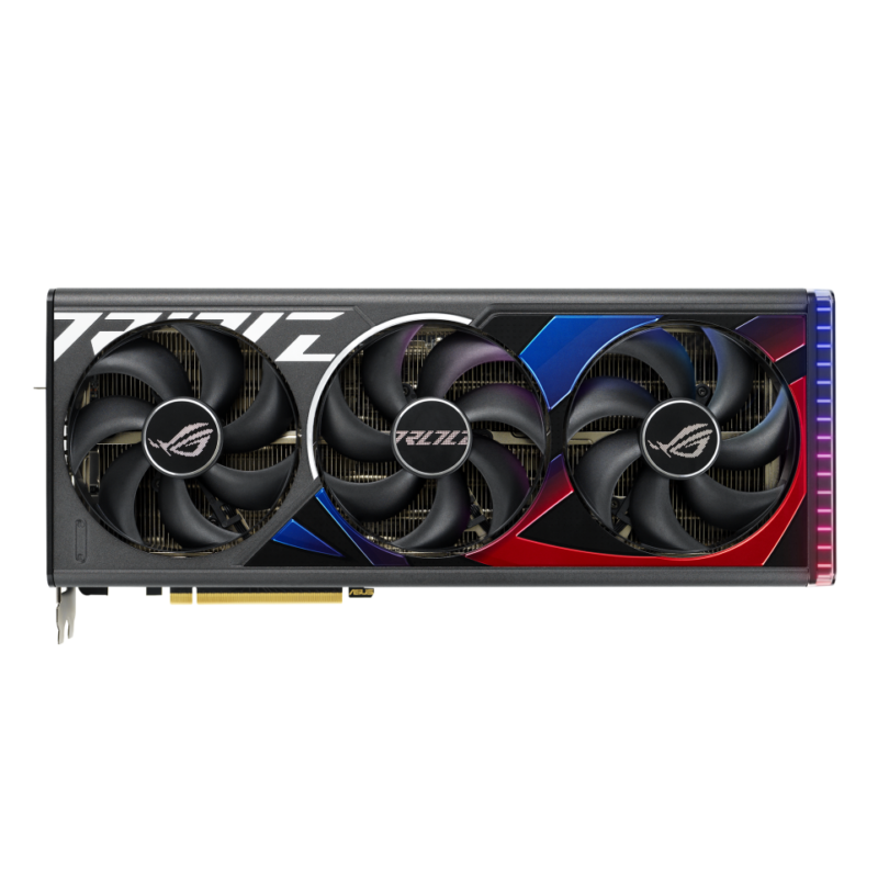 RTX 40 series
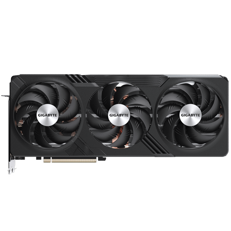 Radoen 7000 series
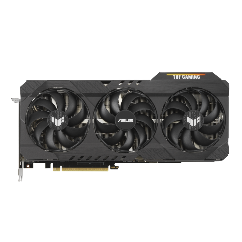 Geforce RTX 30 series
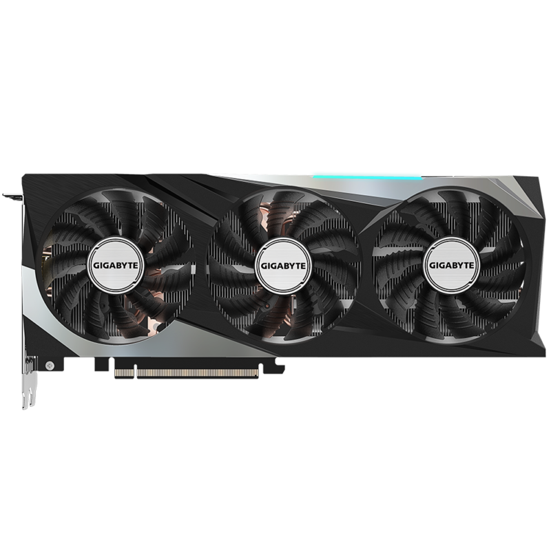 Radoen 6000 series
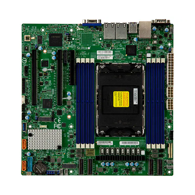 Supermicro Server/workstation
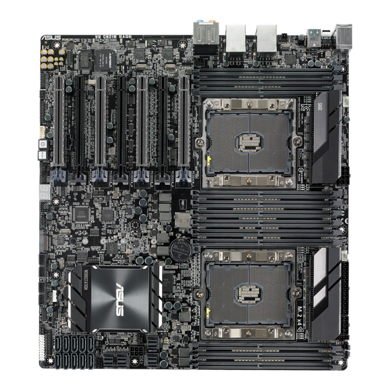 ASUS Server/workstation
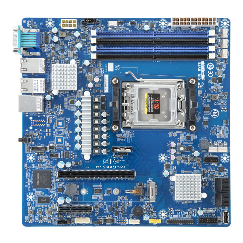 Gigabyte Server/workstation
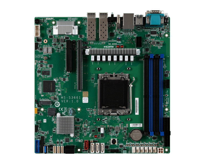 MSI Server/workstation
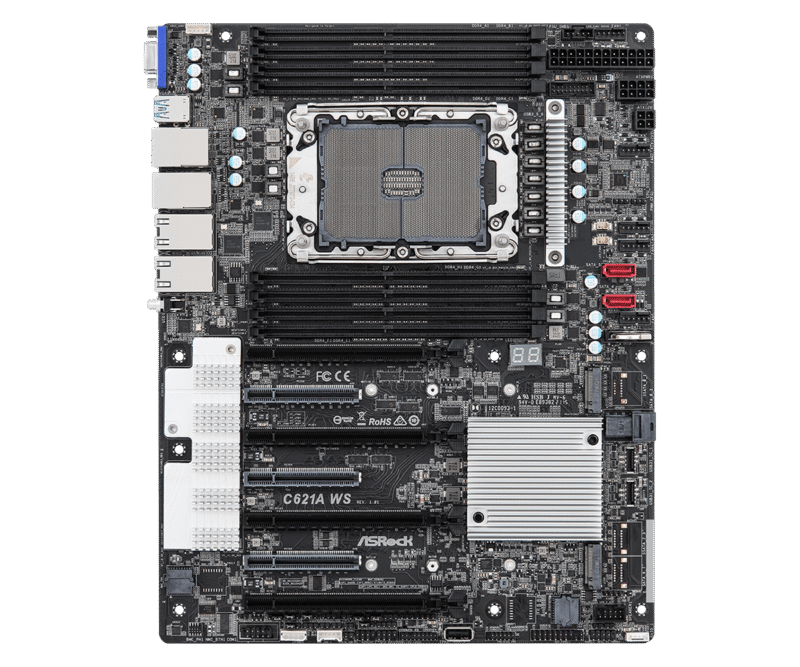 Asrock Server/workstation
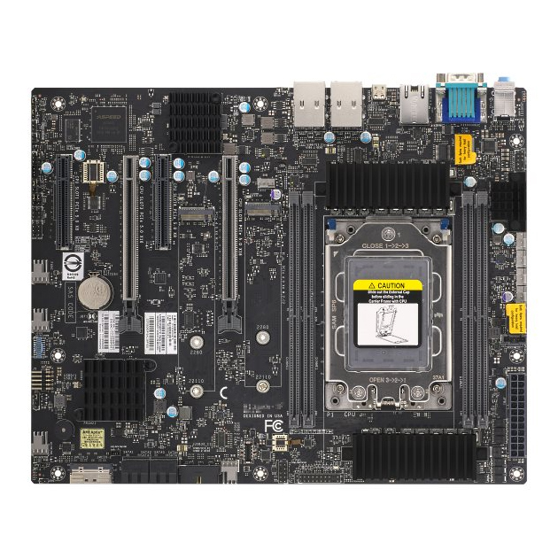 Other Server/workstation
Reviews
There are no reviews yet.